Smart Nano Semiconductor Characterization System

FR1000 by Fronka Tech

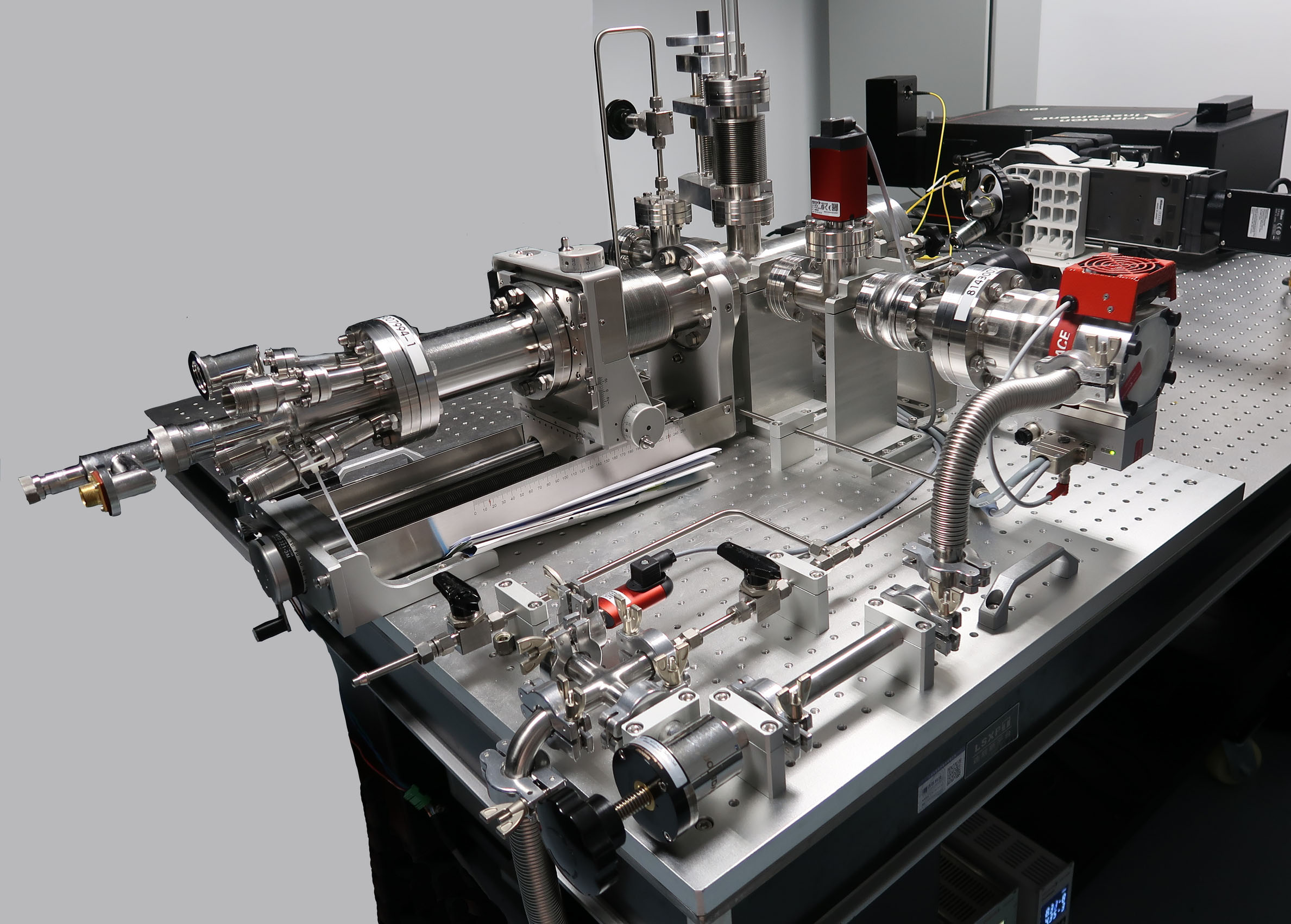
Home–made in-situ FET/MBE system, photoelectrical measurement system in ultra-high vacuum (UHV) with tunable monochromatic light source.

FR1000 is able to conduct in-situ physical properties measurement for nanomaterials. The measuring processes on-site as they are occurring and under changing external stimuli is the paramount goal of in-situ technique with real-timecresponse to the users. Moreover, multiple process can be done within one workstation so that the physical transfer of the sample from one instrument to another can be avoided. The material scope that can be investigated is largely broadenedcto include materials that are easily oxidized upon air exposure.

Fronka Tech is a NUS spin-off company in collaboration with the NUS Industry Liaison Office’s flagship innovation programme GRIP. “Fronka” means “frontier characterization”. We provide advanced characterization solutions for nanomaterial scientists.

fronkatech.com
contact@fronkatech.com, guorui@fronkatech.com

Selected Publications:

  1. "Black Phosphorus Invertor Devices Enabled by in-situ Aluminum Surface Modification"
    Zheng Y, Hu ZH, Han C, Guo R, Xiang D, Lei B, Wang YN, He J, Lai M, Chen Wei*, Nano Res. 12, 531–536 (2019) DOI: 10.1007/s12274-018-2246-y
  2. "Nondestructive Hole Doping Enabled Photocurrent Enhancement of Layered Tungsten Diselenide"
    Lei B, Zheng Y, Hu ZH, Guo R, Xiang D, Liu T, Wang YN, Lai M, He J, Chen Wei*, 2D Mater. 6, 024002 (2019) DOI: 10.1088/2053-1583/ab0708
  3. "Two-dimensional Multi-bit Optoelectronic Memory with Broadband Spectrum Distinction"
    Xiang D, Liu T, Xu JL, Tan JY, Hu ZH, Lei B, Zheng Y, Wu J, Castro Neto AH, Liu L, Chen Wei*, Nat. Commun. 9, 2966 (2018) DOI: 10.1038/s41467-018-05397-w
  4. "Abnormal Near-infrared Absorption in two-dimensional Black Phosphorus Induced by Ag Nanoclusters Surface Functionalization" (Selected as Frontispiece Paper)
    Hu ZH, Li Q, Lei B, Wu J, Zhou QH, Gu CD, Wen XL, Wang JY, Liu YP, Li SS, Zheng Y, Lu JP, He J, Wang L, Xiong QH, Wang JL*, Chen Wei*, Adv. Mater. 30, 1801931 (2018) DOI: 10.1002/adma.201801931
  5. "Non-volatile and Programmable Photodoping in MoTe2 for Photoresist-free Complementary Electronic Devices"
    Liu T, Xiang D*, Zheng Y, Wang YN, Wang XY, Wang L, He J, Liu L, Chen Wei*, Adv. Mater. 30, 1804470 (2018) DOI: 10.1002/adma.201804470
  6. "Direct Observation of Semiconductor-Metal Phase Transition in Bilayer Tungsten Diselenide Induced by Potassium Surface Functionalization"
    Lei B, Pan YY, Hu ZH, Xiang D, Zheng Y, Guo R, Han C, Wang LH, Lu J, Yang L*, Chen Wei*, ACS Nano 12, 2070-2077 (2018) DOI: 10.1021/acsnano.8b00398
  7. "Water-Catalyzed Oxidation of Few-Layer Black Phosphorous in Dark Environment"
    Hu ZH, Li Q, Lei B, Zhou QH, Xiang D, Lyu ZY, Hu F, Wang JL, Ren YJ, Guo R, Goki E, Wang L, Han C*, Wang JL*, Chen Wei*, Angew. Chem. Int. Ed. 56, 9131-9137 (2017) DOI: 10.1002/anie.201705012
  8. "Surface Functionalization of Black Phosphorus via Potassium towards High Performance Complementary Devices"
    Han C, Hu ZH, C. Gromes L, Bao Y, Carvalho A, Tan SJR, Lei B, Xiang D, Wu J, Wang L, Huo FW, Huang W, Loh KP, Chen Wei*, Nano Lett. 17, 4122-4129 (2017) DOI: 10.1021/acs.nanolett.7b00903
  9. "Oxygen Induced Strong Mobility Modulation in Few-layer Black Phosphorus"
    Han C, Hu ZH, Carvalho A, Guo N, Zhang JL, Hu F, Xiang D, Wu J, Lei B, Wang L, Zhang C, Castro-Neto AH, Chen Wei*, 2D Mater. 4, 021007 (2017) DOI: 10.1088/2053-1583/aa59ce
  10. "Largely Enhanced Optoelectronic Performance of Tungsten Diselenide Phototransistor via Surface Functionalization"
    Lei B, Hu ZH, Xiang D, Wang JY, Han C*, Chen Wei*, Nano Res. 10, 1281-1291 (2017) DOI: 10.1007/s12274-016-1386-1
  11. "Surface Transfer Doping Induced Effective Modulation on Ambipolar Characteristics of Few-layer Black Phosphorus"
    Xiang D, Han C, Wu J, Zhong S, Liu YY, Lin JD, Zhang XA, Hu WP, Özyilmaz B, Castro Neto AH, Wee ATS, Chen Wei*, Nat. Commun. 6, 6485 (2015) DOI: 10.1038/ncomms7485
  12. "Tuning the Electronic Properties of ZnO Nanowire Field Effect Transistors via Surface Functionalization"
    Han C, Xiang D, Zheng MR, Lin JD, Zhong JQ, Sow CH, Chen Wei*, Nanotechnology 26, 095202 (2015) DOI: 10.1088/0957-4484/26/9/095202
  13. "Gap States Assisted MoO3 Nanobelt Photodetector with Wide Spectrum Response"
    Xiang D, Han C, Zhang JL, Chen Wei*, Sci. Rep. 4, 4891 (2014) DOI: 10.1038/srep04891
  14. "Electron-Doping-Enhanced Trion Formation in Monolayer Molybdenum Disulfide Functionalized with Cesium Carbonate"
    Lin JD, Han C, Wang F, Xiang D, Qin SQ, Zhang XA*, Wang L, Zhang H, Wee ATS, Chen Wei*, ACS Nano 8, 5323-5329 (2014) DOI: 10.1021/nn501580c
  15. "Plasmonic Enhancement of Photocurrent in MoS2 Field-Effect-Transistor"
    Lin JD, Li H, Zhang H, Chen Wei*, Appl. Phys. Lett. 102, 203109 (2013) DOI: 10.1063/1.4807658
  16. "Modulating Electronic Transport Properties of MoS2 Field Effect Transistor by Surface Overlayers"
    Lin JD, Zhong JQ, Zhong S, Li H, Zhang H, Chen Wei*, Appl. Phys. Lett. 103, 063109 (2013) DOI: 10.1063/1.4818463
  17. "Improving Chemical Vapor Deposition Graphene Conductivity using MoO3: An in-situ Field-Effect-Transistor Study"
    Han C, Lin JD, Xiang D, Wang CC, Wang L*, Chen Wei*, Appl. Phys. Lett. 103, 263117 (2013) DOI: 10.1063/1.4860418